Semiconductors
Camgile offers consultancy services in conventional and emerging semiconductor technologies, including material manufacturing and characterisation, standard and MEMS processing, circuit design and simulation, IC layout and verification, parasitic extraction, packaging, testing, troubleshooting, and system integration.
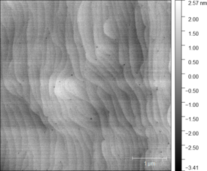
Our materials science understanding puts us ahead of the game in semiconductors design and analysis, having a comprehensive view of the relationship between material and electronic properties. By mastering atomic force microscopy, several material and electronic properties can be visualised and correlated at the nano scale. Electron microscopy complements our range of techniques, with expertise in high-resolution scanning electron microscopy and electron diffration spectroscopy. Past experience in electrochemical and photo-electrochemical etching complements our understanding of semiconductor processing, together with other mechanical and thermal methods. Relevant techniques include AFM, SCM, C-AFM, TUNA, SEM, EDS, optical profilometry, nanoindentation, 3-omega.
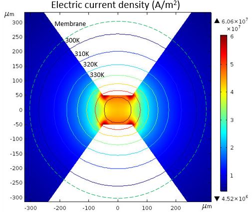
By mastering a full chain of computer-based simulation technology, we save significant development time and expenditure by initial virtual testing and by informing the physical product iterations through building, tuning, and running the relevant numerical models. TCAD simulations (Synopsys Sentaurus) have helped us understand device operation in great detail, analogue simulators (Cadence Virtuoso ADE, SPICE) proved invaluable for assessing circuit performance before manufacturing, while finite-element analysis simulations (COMSOL Multiphysics) revealed the complex inter-dependence between electrical, electromagnetic, mechanical, thermal effects in semiconductors. These are complemented by custom device definitions (SPICE, Verilog-A) and custom scripting (MATLAB, Python, R) depending on the particular challenges.
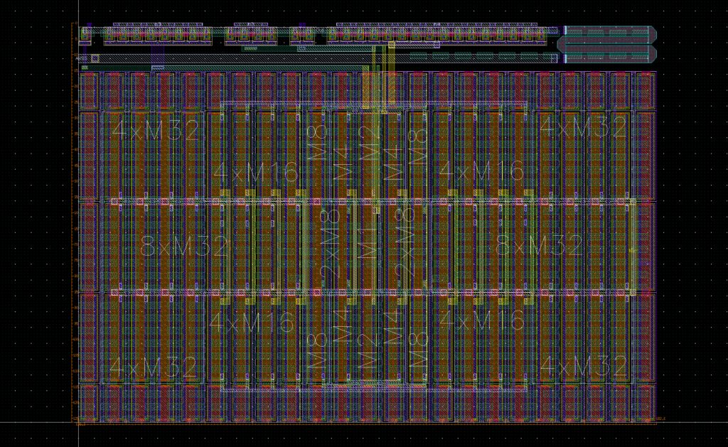
Our materials-to-device experience includes Si CMOS, flexible organic TFT, and GaN technologies, providing superior potential for developing high-performance devices, integrated circuits, modules and products for applications in digital computing, data conversion, sensing, power management, optoelectronics, RF and microwave IC etc.. Full layout projects have been taped out using both manual and automated (Cadence SKILL) layout methods, offering great flexibility between attention to detail in performance-critical aspects and efficiency in performing design routines.

Our expertise spans Analogue – Mixed-Signal – Digital desgin, with a comprehensive view over the specific engineering, performance, applications, and economic challenges of each category. This wide understanding allows the efficient design, validation, testing and debugging of complex circuits in a multitude of semiconductor technologies.
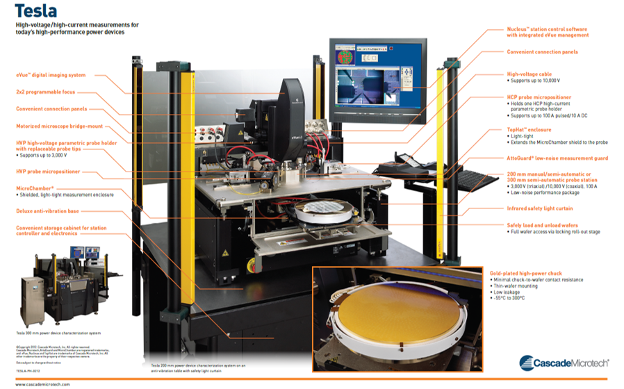
Laboratory testing of wafers, devices and test structures is a key element in the practical validation of electronics and Camgile offers expertise in a wide set of characterisation techniques for unprocessed wafers, bare-die test structures, and packaged devices. These include current-voltage (IV), current-voltage-temperature (IVT), FET characterisation (Id-Vd, Id-Vg) and parameter extraction (Vt, Idssat, gm), capacitange-voltage (CV) and mercury-probe CV (Hg-CV), resistivity and mobility by Hall effect measurements, AFM / SEM / EDS of processed devices. Our expertise covers testing in both manual systems and probe stations and automated production-style systems (Cascade Tesla) with a wide variety of Keithley and Keysight units (SMUs, DMMs, oscilloscopes, signal generators, lock-in amplifiers), including the Keysight B1505A Semiconductor Characterisation System. In the absence of vendor-specific operating environements, Labview can be used for the digital control and interfacing method for complex testing and characterisation operations.